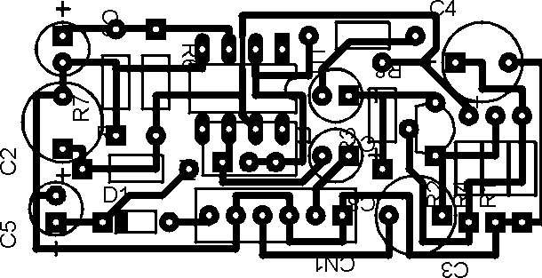
The printed circuit board is one of the most in-demand electronic components for one very simple reason: PCBs are necessary for almost every electronic device to function. As you may already know, modern PCBs are far more evolved than their predecessors, and a small design mistake could send the developer back to the schematic.
If you are developing your first PCB or experimenting with new PCB design techniques, you can save time and prevent headaches by avoiding common mistakes. These six errors happen particularly often, but they are easy to avoid:
Mistake 1: Not Backing up Your Work
This is a common mistake by both novice and professional PCB designers. As about tech explains, an unexpected hardware or software crash could cost you hours or even days of wasted labor if you do not back up your work.
Creating backups has become particularly important due to the widespread use of Electronic Design Automation (EDA) software. Companies such as Circuit Studio produce next-level software to make the development process faster, more organized and more efficient, but you still have to back up your work at regular intervals. Activate the auto-save option in case you forget.
Mistake 2: Not Creating Space by Including Extra Components
Venture Outsource reminds developers to include extra components that may be necessary. If you fail to do this and you later find out that the design needs another component, you won’t have room for the addition. Even if you do not use the extra components, they are easy to remove before fabrication.
Mistake 3: Routing Your Traces Too Close to Plated Through Holes
One of the most important considerations when designing a board is the minimum spacing allowance. Your spacing should account for maximum allowable mis-registration combined with maximum etch back, also known as “manufacturing tolerance buildup.”
If you remove nonfunctional pads from a layer and you route a trace between plated through holes on that layer, the trace can short out during testing and destroy the unit.
Mistake 4: Not Considering the Thickness of Copper
If you are not specific about the thickness of copper, then there may not be adequate plating in the holes. On most PCBs, the final thickness of the copper is 1 to 2 ounces per square foot.
Mistake 5: Not Incorporating the Appropriate Edge Tolerances
If your PCB does not have the appropriate edge tolerances, there could be a short with the cases and metal chassis. As a rule of thumb, your traces and ground plates should end 0.01 inches from the board edges.
Mistake 6: Not Getting Reviews of Your PCB Design
This mistake is particularly common among amateur developers. You should never underestimate the valuable insight of an experienced technician. A veteran PCB designer will be better able to identify problems that will arise when your printed circuit board enters fabrication.
These reviews should cover:
- An evaluation of initial placement of components (do this after creating the schematic);
- An evaluation of the routing layers in hard copy (do this after you complete the routing);
- And an evaluation of the assembly data package and fabricated PCB (do this before you send out the package).
Getting reviews for your PCB design is particularly important if there are several stakeholders in the product you are creating. The reviews will let you incorporate their input before sending out the package.
If you do not have access to these resources, you should at least consult a technician to review your schematic and routing. An extra pair of eyes can help you identify subtle oversights that could affect the function of your printed circuit board.
Although there are countless ways to make a mistake when developing a printed circuit board, you can avoid most oversights by following these six tips. Take the time to prepare adequately, be specific about your dimensions and parameters, and ask for reviews throughout development.
